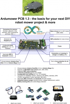
PCB 1.3 (English)
This page describes how to assemble PCB 1.3, how to add modules and how to configure the PCB. The PCB and all required modules can be purchased as complete kits via the shop ![]() .
.
NOTE: WE ARE CURRENTLY WORKING ON THIS PAGE - PLEASE LOOK AT PCB 1.2 FOR MISSING INFORMATION
Inhaltsverzeichnis
Specifications
PCB size: 272mm x 115mm
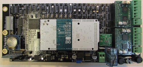
Schematics, Drawings, Photos
Videos
- Assembly part 1 (jumper, capacitors (power), INA, jumper power, bargraph, bluetooth, jumper I2C bus)
- Assembly part 2 (motor drivers)
- Assembly part 3 (Arduino, protection, MOSFET, fuse holder, relay)
- Assembly part 4 (back side: odo-divider, power connectors, buzzer, resistors, capacitors)
- Assembly part 5 (sensor jumpers, connector sockets)
- Assembly part 6 (Capacitors motor output stage )
- Assembly part 7 (Placing into operation)
Checklist
- only set jumper JP1 (9V power) after you have manually set and measured the correct voltage (9v) at DC/DC Vout pin
- set jumper JP13 on PCB back side for a Marotronics Arduino Due (i.e. Due clone) for automatic reset
- set jumper JP12 (GPS signal voltage) to 3.3VP for Marotronics GPS module
- set jumper JP7 (GPS operating voltage) to 5VP for Marotronics GPS module
- set jumper JP10 (Bluetooth signal voltage) to 3.3VP for Marotronics Bluetooth module
- set jumper JP4 (Bluetooth operating voltage) to 5V for Marotronics Bluetooth module
- set jumper JP6 (WIFI operating voltage) to 3.3V for Marotronics WIFI module
- set jumper JP11 (WIFI signal voltage) to 3.3V for Marotronics WIFI module
- set jumper JC2 (IMU signal voltage) to 3.3V for Marotronics IMU module
- only set I2C jumpers JC2, JC3, JC4, JC5, JC6, JC7 (at the top) if there is a corresponding I2C module installed
- set jumper JP8 to 'Always-ON' for tests and for Arduino uploads, for regular operation (and automatic undervoltage power-off) to 'Automatic'
- unset jumper JP3 (2nd mower motor MC33926 M1FB), not used
- RTC module must be installed for proper I2C bus operation
- press button P20 to power-on PCB
Assembly
The assembly of the board is tricky as some components have been packed tightly - especially those below the motor drivers.
The following table lists each component to be placed by hand along with other components that might collide. Collisions marked with a '?' are hard (but still possible) to solder if the components are not placed in the right order. Those without a '?' are impossible.
TODO: sort table by dependencies and solderability
TODO: give advice what to do with components that ultimately block each other
| Component | Can be blocked by | Can block |
|---|---|---|
| BY1 | Dual2, PRFA2 | RL1? |
| BY2 | Dual2, C11?, RL3? | RL3 |
| BY3 | Dual2, PRFA2 | RL1 |
| BY4 | Dual2, PRFA2? | |
| BY5 | Dual1, CC2? | RL2 |
| BY6 | Dual1, P49 | RL2 |
| BY7 | Dual1, CC2? | |
| BY8 | Dual1, CC2, RL2? | |
| BY9 | Dual1, PRFA1, C10? | |
| BY10 | Dual1, Dual2, PRFA1, CC3, RL3? | CC3? |
| BY11 | Dual2, C11? | RL3 |
| BY12 | Dual2, RL3?, PRFA1? | CC3 |
| C1 | F1? | |
| C2 | Due? | |
| C3 | U3 | |
| C8 | ||
| C9?? missing? | Due? | |
| C10 | Dual1, PRFA1?, Dual1_Pins? | Dual1_Pins, Due_Pins?, P31?, RL3, U3?, BY9? |
| C11 | Dual2, Dual2_Pins? | DKE2?, Dual2_Pins, P1?, P2?, P19?, P21?, P41?, P46?, PRFA2?, RL1?, BY2?, BY11? |
| C12 | U1 | |
| C13 | ||
| CC1 | Dual2 | |
| CC2 | Dual1 | DKE1, BY5?, BY7?, BY8? |
| CC3 | Dual1, Dual2, EF3, BY12, BY10? | EF3, BY10 |
| D1 | ||
| D9 | ||
| D10 | K3 | |
| D73 | ||
| DKE1 | Dual1, CC2, RL2? | |
| DKE2 | Dual2, C11? | RL1 |
| Dual1 | EF3, PRFA1, RL2, RL3, BY5, BY6, BY7, BY8, BY9, BY10, C10, CC2, CC3, DKE1, P49?, Dual1_Pins | |
| Dual2 | PRFA2, RL1, RL3, BY1, BY2, BY3, BY4, BY10, BY11, BY12, C11, CC1, CC3, DKE2, Dual2_Pins | |
| Dual1_Pins | C10, Dual1 | C10? |
| Dual2_Pins | C11, Dual2 | C11? |
| Due | Due_Pins?, JP13?, SP2?, C2?, C9? | |
| Due_Pins | Due?, C10? | |
| EF1 | P49? | |
| EF2 | ||
| EF3 | Dual1, PRFA1?, CC3 | CC3 |
| F1 | JP1?, C1? | |
| I2C1 | ||
| I2C2 | ||
| I2C3 | ||
| I2C4 | ||
| I2C5 | ||
| I2C6 | ||
| I2C7 | ||
| JC2 | ||
| JC3 | ||
| JC4 | ||
| JC5 | ||
| JC6 | ||
| JC7 | ||
| JP1 | F1? | |
| JP2 | ||
| JP3 | P22, P4 | |
| JP4 | ||
| JP5 | ||
| JP6 | ||
| JP7 | ||
| JP8 | ||
| JP9 | ||
| JP10 | ||
| JP11 | ||
| JP12 | ||
| JP13 | Due? | |
| K3 | D10 | |
| P1 | C11? | |
| P2 | C11? | |
| P3 | ||
| P4 | JP3 | |
| P5 | ||
| P6 | ||
| P7 | ||
| P8 | SP1 | SP1? |
| P9 | ||
| P10 | ||
| P11 | ||
| P12 | ||
| P13 | ||
| P14 | ||
| P15/P16/P18 | ||
| P17/P39/P36 | ||
| P19 | C11? | |
| P20 | ||
| P21 | C11? | |
| P22 | JP3 | |
| P23 | ||
| P24 | ||
| P25 | ||
| P26 | ||
| P27 | ||
| P28 | ||
| P29 | ||
| P30 | ||
| P31 | C10? | |
| P32 | ||
| P33 | ||
| P34 | ||
| P35 | ||
| P37 | ||
| P38 | ||
| P40 | ||
| P41 | C11? | |
| P42 | ||
| P43 | ||
| P44 | ||
| P45 | ||
| P46 | SP1, C11? | SP1? |
| P47 | ||
| P48 | ||
| P49 | Dual1?, EF1? | RL2, BY6 |
| P50 | U2? | |
| P51 | ||
| PRFA1 | Dual1, RL2 | RL2, RL3, BY9, BY10, BY12?, C10?, EF3? |
| PRFA2 | Dual2, RL1, C11? | BY1, BY3, BY4? |
| Q2 | ||
| Q4 | ||
| RL1 | Dual2, BY3, DKE2, BY1?, C11? | PRFA2 |
| RL2 | Dual1, P49, BY6, BY5, PRFA1 | BY8?, DKE1?, PRFA1 |
| RL3 | Dual1, Dual2, C10, BY2, BY11, PRFA1 | BY2?, BY10?, BY12? |
| S1 | ||
| S2 | ||
| S3 | ||
| SP1 | P8?, P46? | P8, P46 |
| SP2 | Due? | |
| U11 | ||
| U1 | C12 | |
| U2 | U8RTC?, P50? | |
| U3 | C10? | C3 |
| U8RTC | U2? |
Forum
http://www.ardumower.de/index.php/de/forum/ardumower-pcb/1348-building-instruction-for-the-1-3-board

